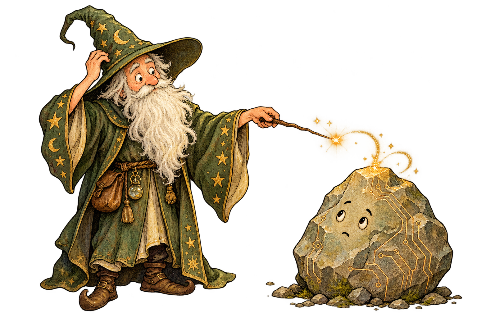
The invisible machinery behind everything
Your phone. Your car. The equipment in a hospital. The robots in a factory. Much of the machinery we depend on runs on chips: tiny circuits built on silicon, an element found in ordinary rocks. Those circuits process information, store it, and help control what happens next. [1]
We usually see the screen or the finished product. Underneath it is a material we pulled from the ground and taught to do useful work. So how does silicon go from being part of a rock to being part of a computer?
First, why silicon?
Silicon is everywhere around us, usually bonded to other elements. It makes up about 27.7% of Earth's crust by mass, second only to oxygen. Quartz is silicon dioxide, and silicon is also part of the silicate minerals that make up so much of the rock beneath our feet. [2]
Swedish chemist Jöns Jacob Berzelius is generally credited with isolating silicon in 1824. People had been using its compounds for far longer; separating out the element was a different challenge. [2]
What makes silicon useful for chips is that it's a semiconductor. We can deliberately change its electrical behavior by adding tiny amounts of other elements, then build structures that control current. That control is where computing starts. [1]
Turning rock into something absurdly pure
Silicon dioxide has to be reduced to silicon. The resulting silicon still contains too many impurities for chipmaking and needs further purification. [2]
One established route converts the raw silicon into a compound called trichlorosilane. It can be purified by distillation, separating unwanted substances before silicon is deposited back into solid form. The result is high-purity polysilicon: silicon made up of many crystals. WACKER, a major producer, uses this chemical purification process to make high-purity polysilicon. [3]
After purification, the next step is to grow the silicon into a single crystal.
Growing a crystal by pulling it out of a furnace
This is one of the coolest parts. In the Czochralski process, purified silicon is melted in a quartz crucible. A small seed crystal touches the surface. The seed is slowly lifted and rotated, and silicon solidifies onto it with the same crystal orientation. Temperature and pulling speed help control the shape of the growing crystal. [4]
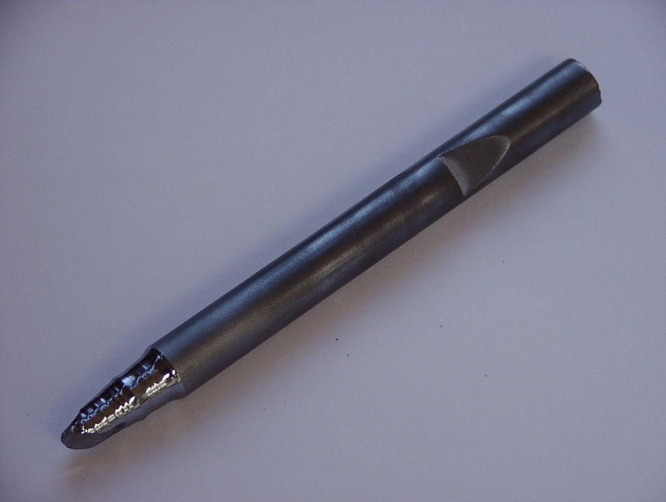
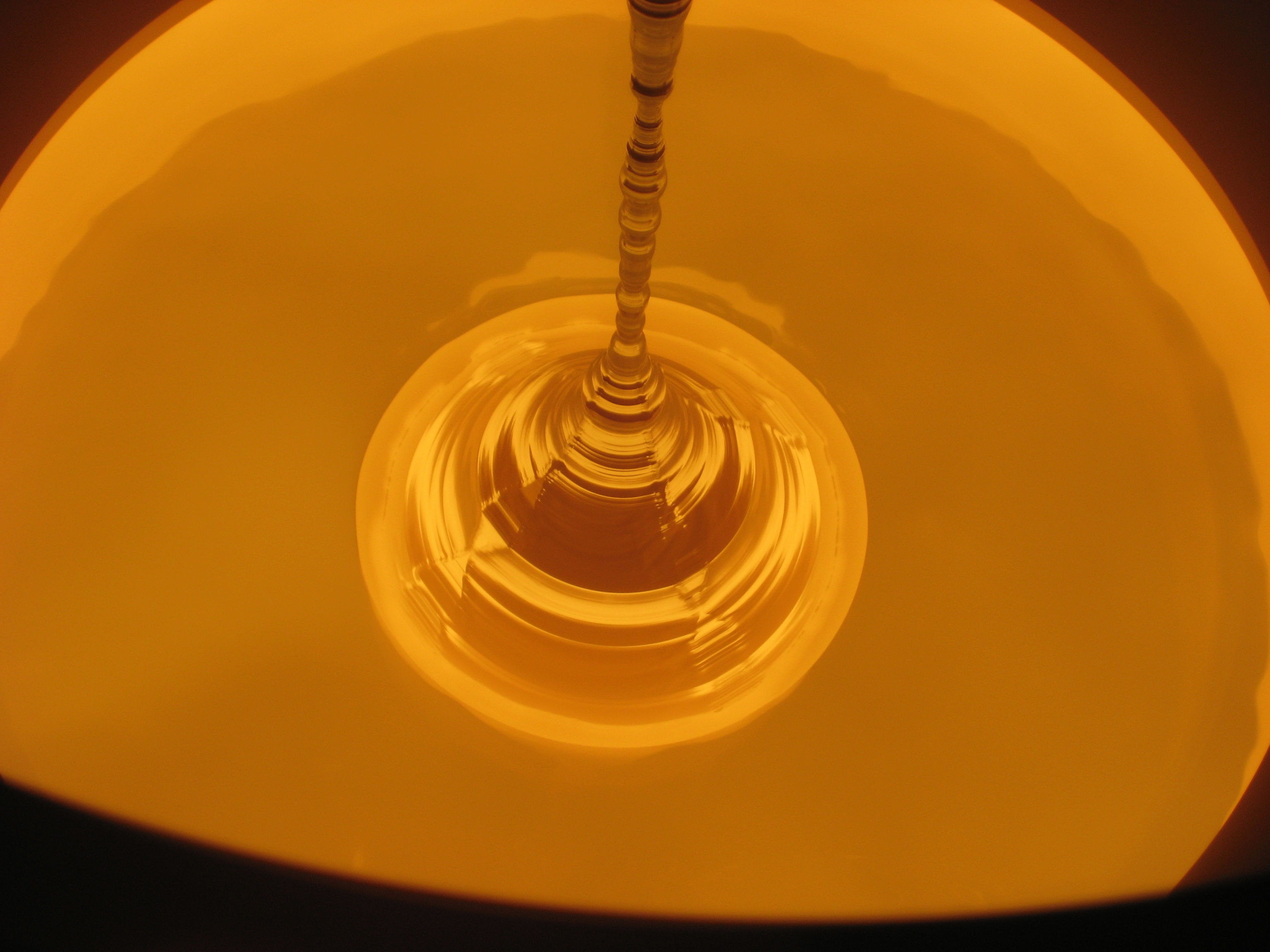
The result is a large single crystal called an ingot or boule. That skinny connection at the top makes it look like a metallic weight hanging from a string. As the seed is pulled upward, more silicon solidifies beneath it, extending the crystal.
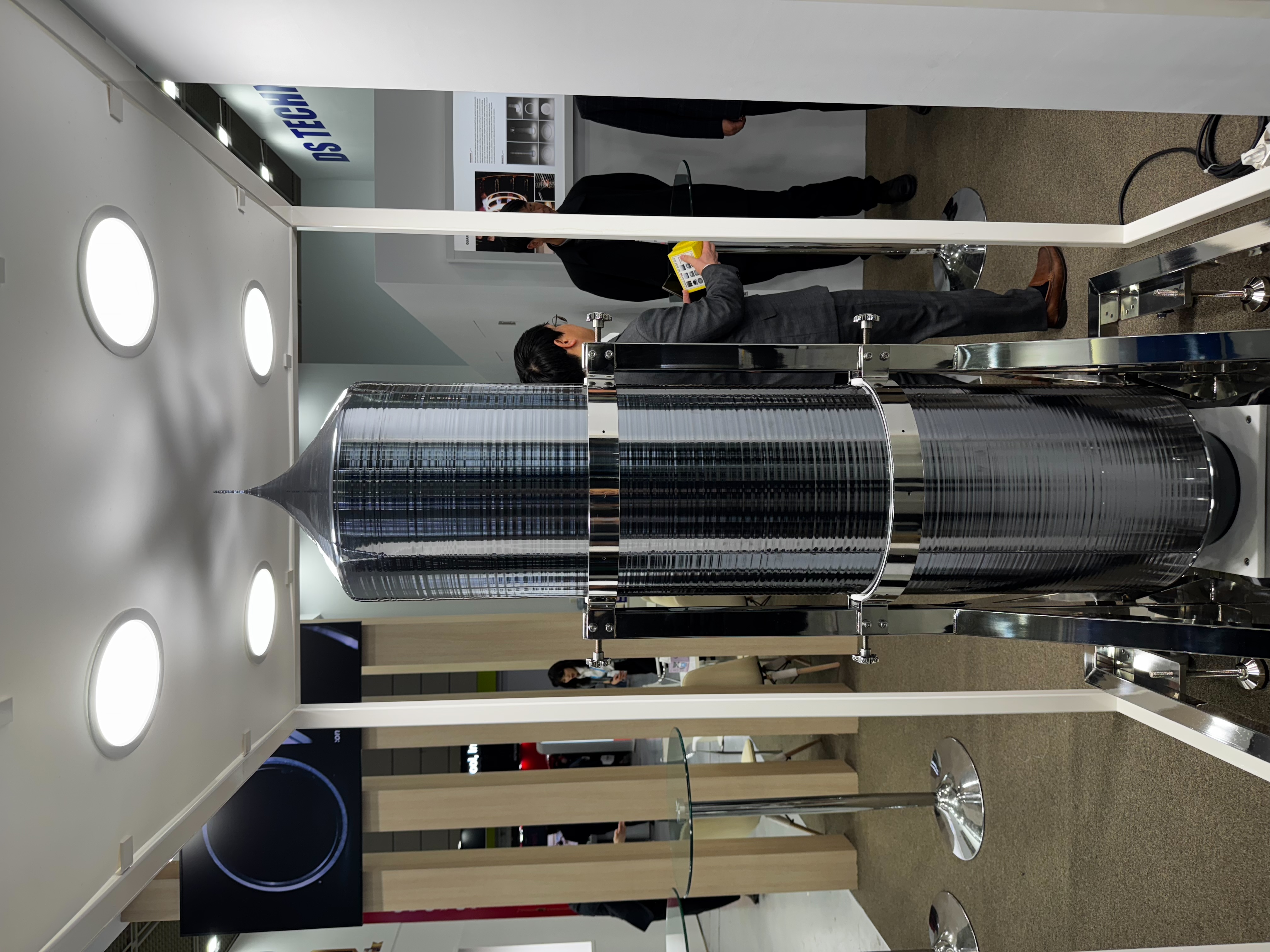
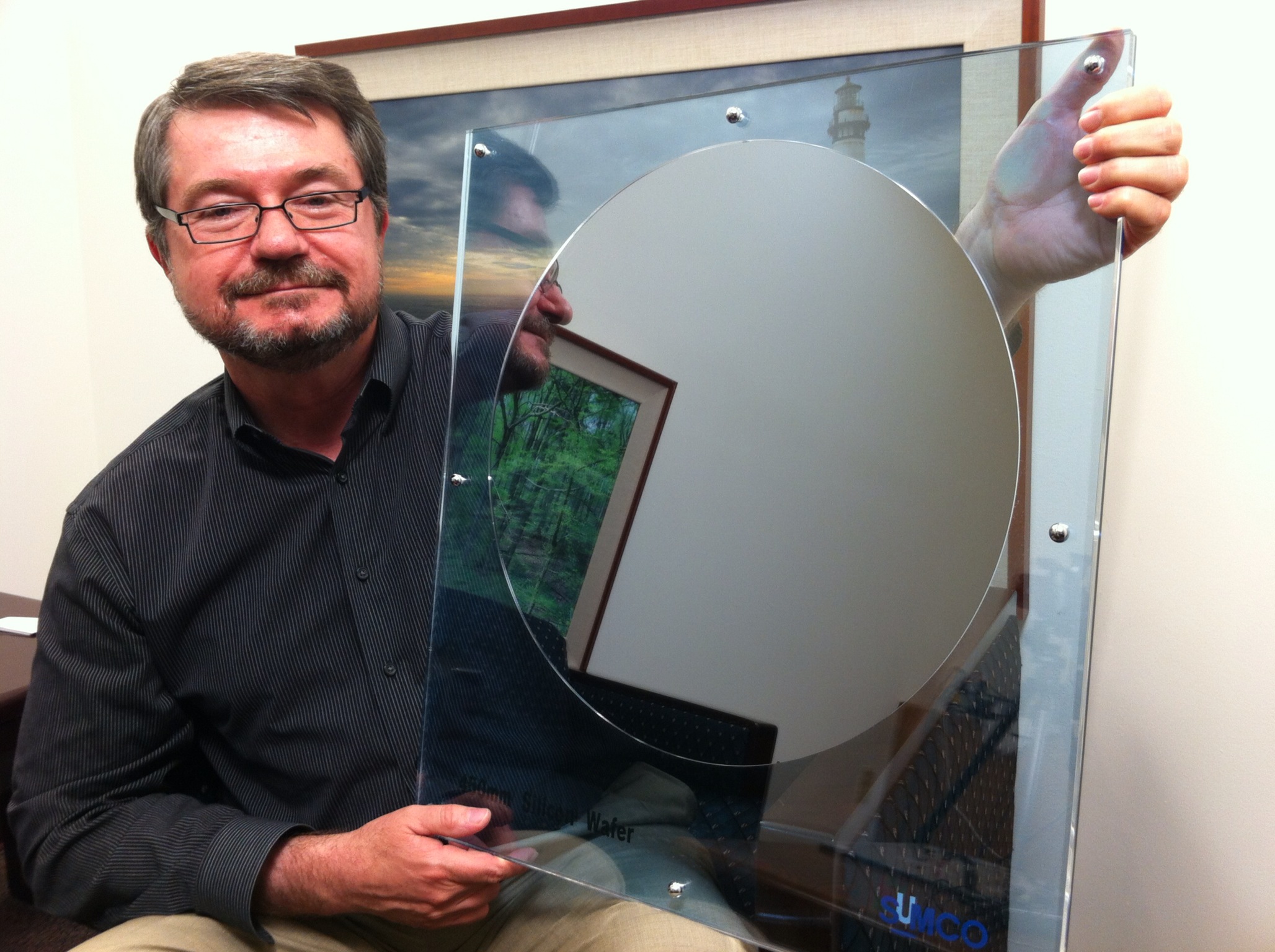
The ingot is then sliced into thin discs. Those discs are flattened, etched, polished, cleaned, and inspected to become wafers. At this point we've made an extremely precise starting surface. The circuitry still has to be built. [4]
How a piece of silicon does anything
In a digital chip, transistors act as tiny electrically controlled switches. Circuits use distinguishable electrical states to represent zeros and ones. Connect switches in the right arrangements and you can perform logic; combine those circuits and you can process and store information. Advanced chips contain billions of transistors. [1]
We design the physical structures and the instructions that let these circuits perform useful work.
But we didn't start with billions of switches on a chip. We started with individual components we could hold in our hands.
From wiring transistors to printing with light
Early transistor circuits were assembled from separate parts. Each transistor was a physical component, mounted on a circuit board and connected to other components through its leads. Building a more capable computer meant fitting together more parts and more connections. [12]
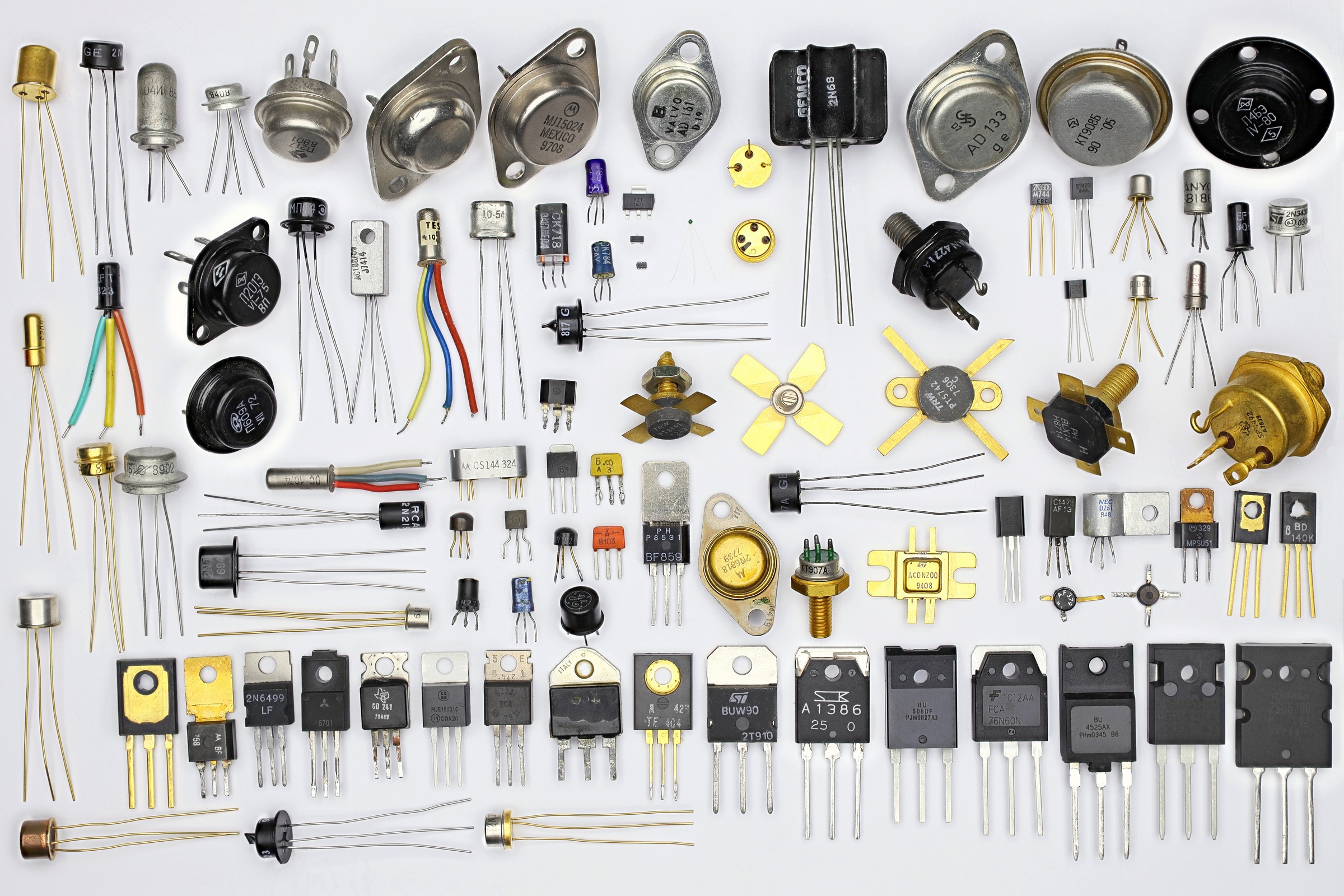
The huge leap came in the late 1950s with the integrated circuit: forming multiple components together in one piece of semiconductor material. Transistors could be formed in silicon and connected with metal lines deposited over an insulating layer. Instead of mounting each transistor separately, we could manufacture a whole circuit as a chip. [13]
So how do you make all those tiny structures in the right places? Light was already becoming part of the answer. In the 1950s, researchers adapted photographic patterning techniques to semiconductor manufacturing. A mask and a light-sensitive coating let them define small openings where the silicon would be processed. [14]
That's the shift: from assembling a circuit out of separate transistors to manufacturing its transistors and connections together, with light defining the patterns. The decades since have been about making those patterns smaller, more precise, and repeatable enough to produce chips in enormous numbers.
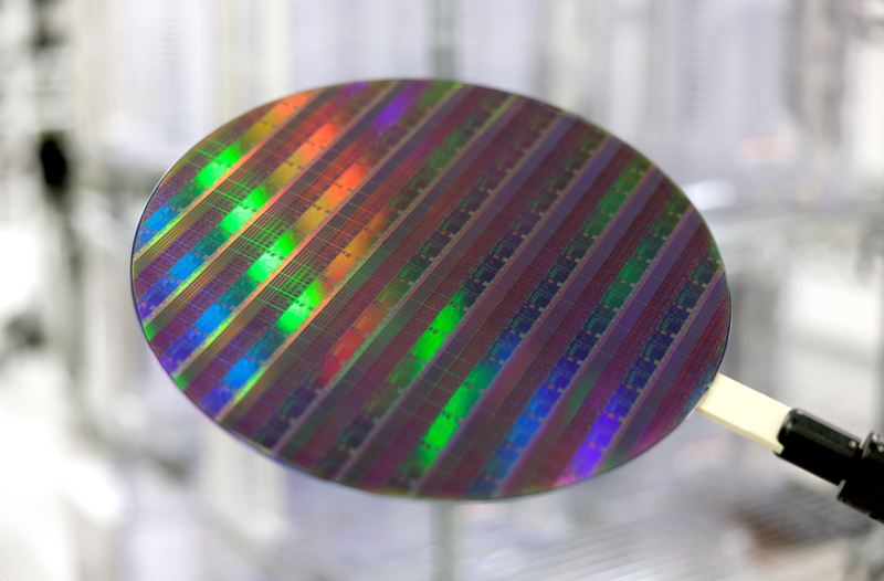
Photolithography transfers a pattern onto a wafer coated with a light-sensitive material called photoresist. Exposure changes the resist's chemistry. Developing it leaves a pattern that guides later manufacturing steps, such as etching away material. Other steps add layers or alter the electrical properties of selected regions. [5]
A chip is built through many repeated steps, with patterns aligned across layers. Lithography supplies the patterns that guide the next manufacturing steps. [6]
How did transistors get so small?
The big change was building the switches together in the silicon. A separately packaged transistor needs a case and connections large enough to handle. Inside a processor, each transistor shares the chip's protection and connects through microscopic metal wiring. The transistor itself is still a physical device; it just no longer needs an individual case and long external leads. [17]
Then decades of manufacturing improvements reduced the size of the working structures. Better optics, shorter-wavelength light, and techniques that split fine patterns across multiple processing steps helped define smaller features. More precise etching, deposition, and doping turned those patterns into working devices. We manufacture enormous numbers together across a wafer, with each step acting on the patterned surface. [5] [18]
The switch's shape changed too. In a MOSFET, a voltage on a terminal called the gate controls current through a semiconductor channel. As that channel gets shorter, keeping the switch fully off becomes harder. FinFETs raise the channel into a fin so the gate can control it from three sides. Gate-all-around designs surround the channel, improving control further. Smaller patterns and better electrical control work together to fit more useful switches into the same area. [17] [19] [20]
The basic idea is straightforward. Making it work at the scale of modern chips takes some extraordinary equipment. That brings us to ASML.
ASML: engineering at the edge of possibility
ASML is a Dutch company that designs and builds the lithography machines chipmakers use to pattern wafers. Its headquarters are in Veldhoven, in the Netherlands. Its job is to build the equipment that transfers a circuit's design onto silicon with extraordinary precision. [15]
The company began in 1984 as a joint venture between Philips and ASM International, under the name ASM Lithography. Its first home was a shed near Philips in Eindhoven. It moved to Veldhoven in 1985 and became an independent public company in 1995. From those beginnings, it spent decades developing machines that could print ever finer patterns. [16]
Why does the kind of light matter?
Light behaves as a wave. The distance between successive peaks is its wavelength. Shorter wavelengths help a lithography machine distinguish finer details, allowing chipmakers to fit smaller structures onto a wafer.
EUV stands for extreme ultraviolet, a kind of light we can't see. ASML's EUV machines use a wavelength of 13.5 nanometers; a nanometer is one billionth of a meter. That's more than fourteen times shorter than the 193-nanometer light used in many deep ultraviolet (DUV) machines. The wavelength describes the light, rather than the size of every transistor it can help make. [7]
Chipmakers use EUV for some of the most intricate layers of advanced chips, while DUV handles other layers. Getting EUV into factory production took years: ASML shipped a prototype in 2010, and by early 2020 it had entered high-volume manufacturing. [8] [16]
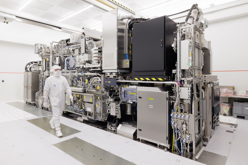
So what does this machine actually do? It makes EUV light, guides that light through a circuit pattern, and projects the pattern onto the wafer's light-sensitive coating. Each part of that journey creates a different engineering problem.
1. Make the light
First, the machine needs an EUV light source. It sends tiny droplets of molten tin through a chamber. One laser pulse flattens a droplet; a stronger pulse turns it into plasma, a hot, ionized state of matter that emits EUV light. This happens 50,000 times a second. All that machinery just to produce the light we'll use to draw the pattern. [7]
The laser system has to deliver enough energy, reliably, to keep this process going. A specialist supplier, TRUMPF, provides the powerful laser-amplifier technology. [9]
2. Guide it without losing the detail
Now we have the light. But air and glass absorb EUV, so it can't travel through an ordinary lens system. The machine keeps its light path in a vacuum, with the air removed, and uses specially coated mirrors to direct it. [10]
This is where ZEISS comes in. The optics company makes the precision mirrors used in ASML's EUV systems. The two companies have worked together since 1986. Their partnership matters here because producing the light is only useful if the mirrors can guide it without distorting the pattern. [10] [16]
Even tiny errors in a mirror's shape can spoil the image. ZEISS puts the required precision in perspective: if an EUV mirror were enlarged to the size of Germany, its largest unevenness would be just 0.1 millimeters high. An entire country's worth of surface, with the biggest imperfection measured in tenths of a millimeter. [11]
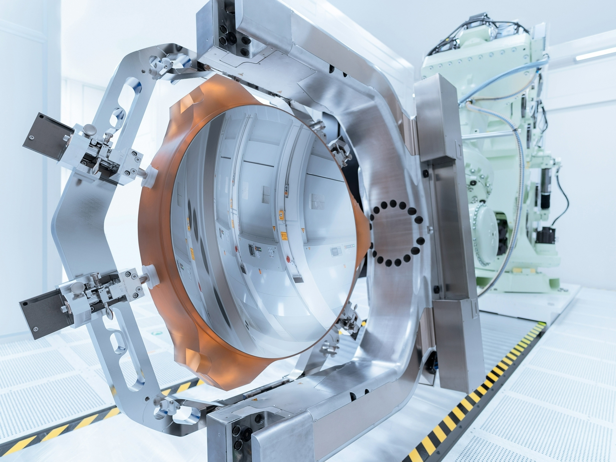
The coating matters too. Alternating layers of silicon and molybdenum make reflections reinforce one another, allowing the mirror to reflect up to 70% of the EUV light. Some light is still lost at every reflection, which makes the shape, coating, and alignment of each mirror essential. [11]
3. Transfer the pattern to the wafer
The circuit pattern is carried on a reflective mask called a reticle. Light reflects from this mask, and the mirrors project a smaller image of its pattern onto the wafer. The wafer is covered in photoresist, the light-sensitive coating introduced earlier. Exposure changes that coating's chemistry, recording the pattern. [8] [5]
Developing the coating reveals the pattern for subsequent processing. Etching, adding material, and changing selected regions' electrical properties build the actual structures. Repeating these steps, with each new pattern aligned to the previous layers, creates the transistors and connections that make the chip work. [5] [6]
Simplified EUV path. Exposure records the pattern; further processing builds the chip's structures.
And this all started with rocks
Once the wafer's circuits have been built, the individual chips are separated, tested, and packaged so they can connect to the rest of a device. This is the finished form most of us recognize. [6]
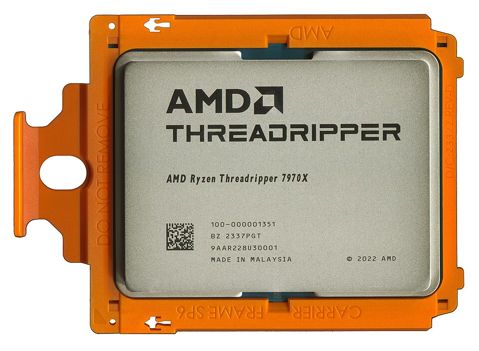

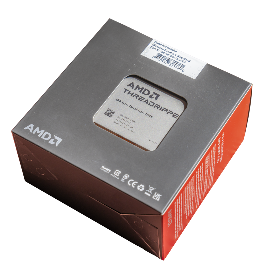

Take an abundant element. Purify it. Grow it into a crystal. Slice it into wafers. Build tiny switches and the connections between them, using manufacturing equipment that sounds made up even when you understand what it's doing.
That's the part that gets me. We can casually pull a phone out of a pocket because people figured out every one of these steps, and then figured out how to repeat them reliably.
Calling it modern day magic might be an understatement.